|
PCB Layout
As I've said before, I only ever built this as a bunch of wires soldered to the back of the DIL socket for the IC, so I've no idea if this layout is any good. Again,click for full-sized versions.
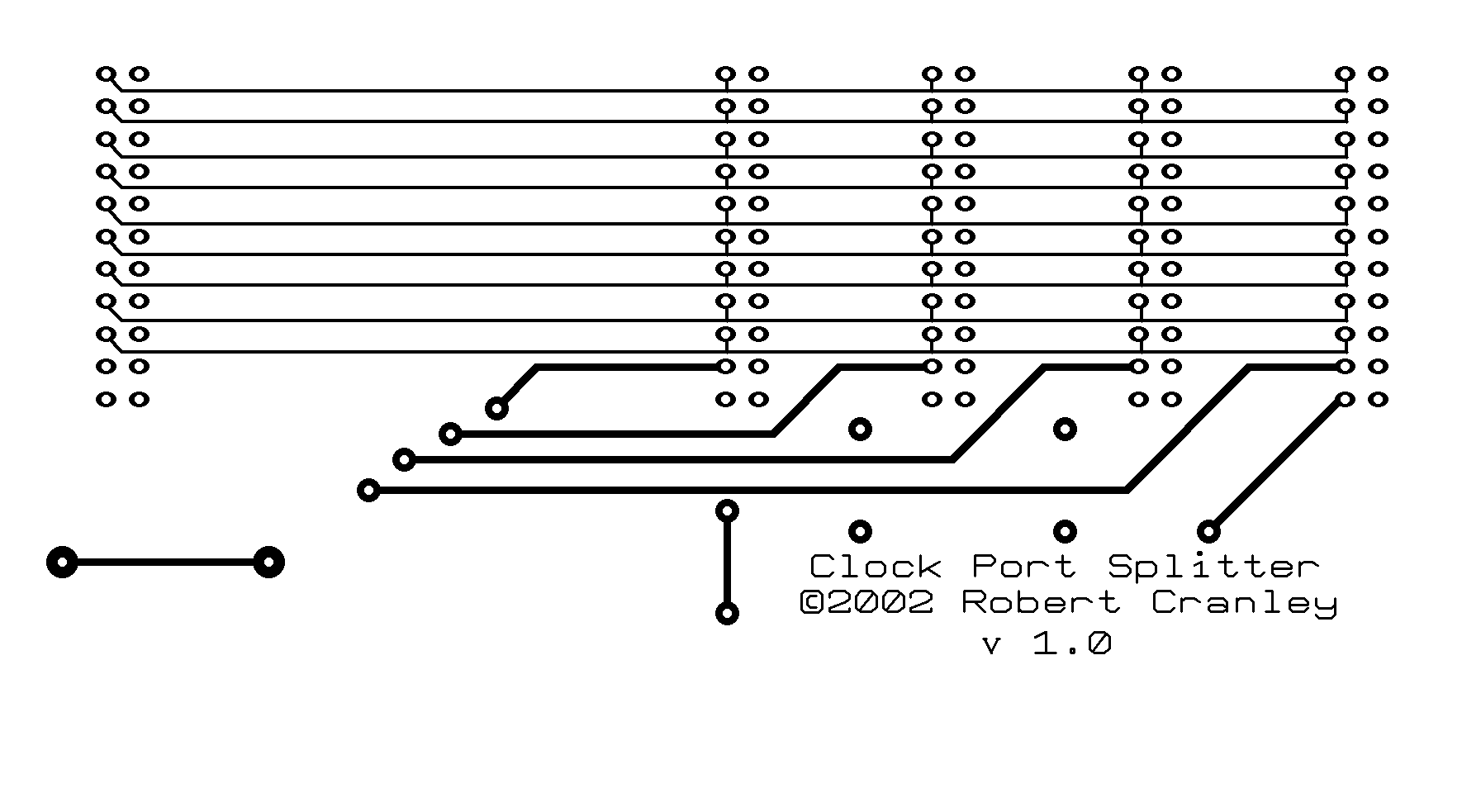 Component side layout Component side layout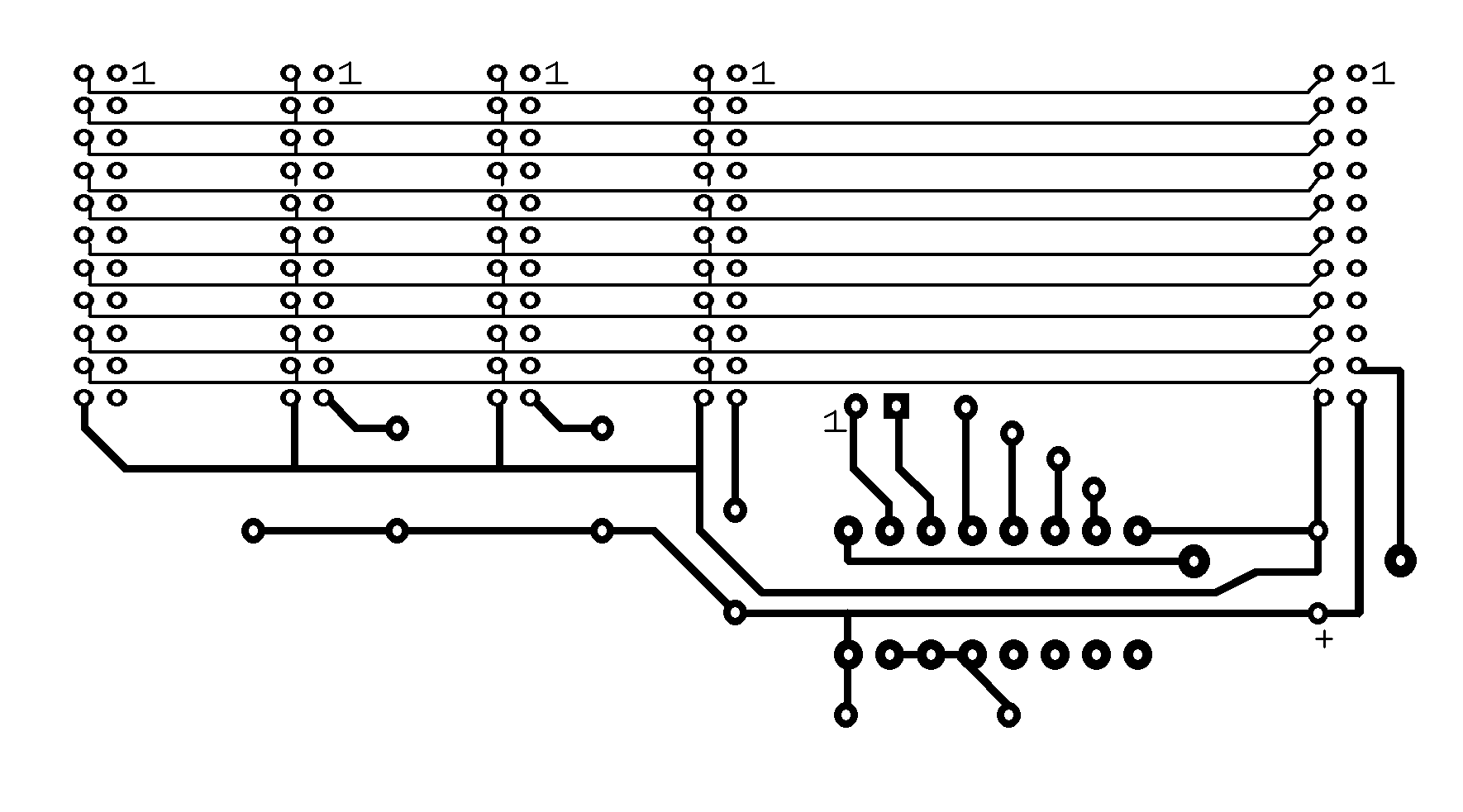 Solder side layout Solder side layout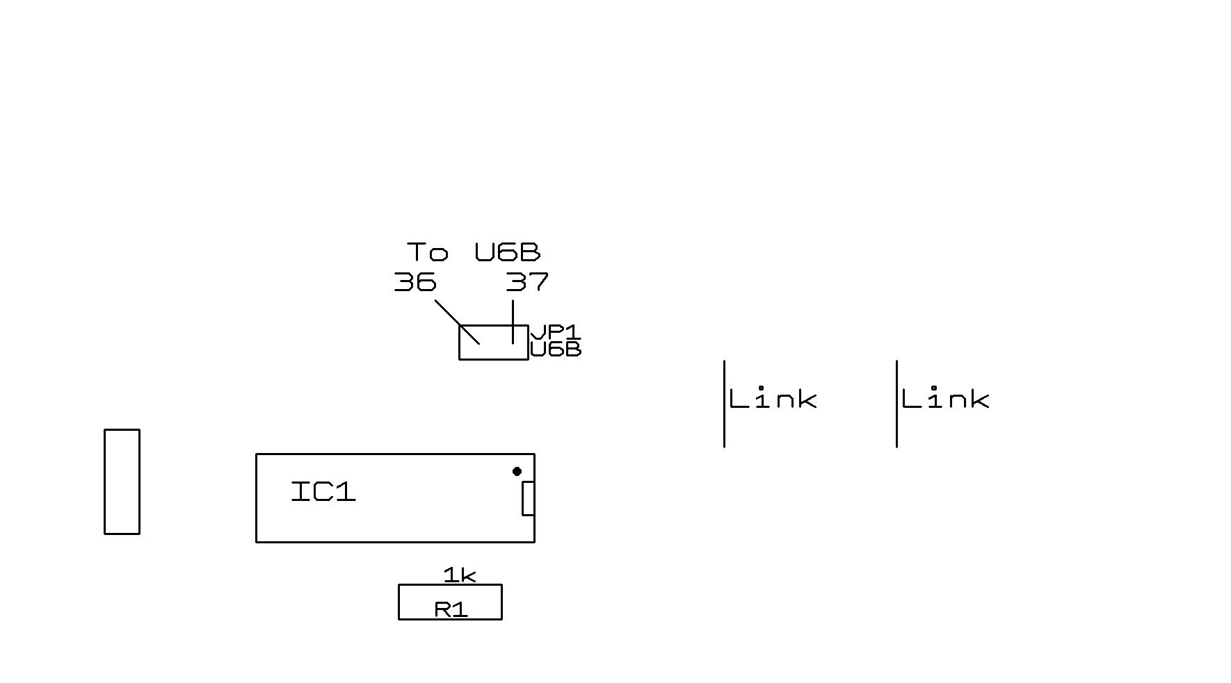 Component side printing Component side printingIt's not finished, as the capacitors are missing for each of the new ports, but apart from that it looks alright. The designed dimensions are 90mm x 50mm, just in case anyone wants to try and prototype them, all holes should be through soldered as both sides of the board have traces, and the printing is optional, but have a look anyway as it shows polarities and where some links are required.
Please let me know if you do end up building this, I'd be interested to hear how you get on!! You can contact me here.
|

|
